

For the past couple of years, I have been powering my Sony 55” LCD TV and charging a couple of laptop computers from a 12V solar system.
Both the Sony TV and the laptop computers have an input voltage of 19.5VDC. To step up the voltage from the battery, I purchased two “LTC3780 Automatic lifting pressure constant voltage step up step down 10A 130W” a.k.a. LTC3780 – High Efficiency, Synchronous, 4-Switch Buck-Boost DC-DC Converters from ebay. These boards operated from a moderately wide 5 – 36V input and had an output voltage range of 1 – 30V.
The LTC3780 has no output current limiting or Undervoltage Lockout (UVLO) on-chip, so the designers of these modules implemented their own using a commodity LM358 OpAmp.
Within the first couple of months, I managed to blow both boards up with the same fault – a very stressed LM358 which would then kill the LTC3780 by exceeding the RUN pin’s absolute maximum voltage. More on this can be found on my wiki here.
In the end, I replaced the LTC3780 I.C. (it cost more than the boards from ebay, but helped with the root cause investigation), omitted the LM358 and used a 0603 resistor between pads of the LM358 to tie the LTC3780’s run pin high. They have operated flawlessly since, albeit without current limiting or low voltage cut-out.
Besides the important low-voltage cutout, I have always wanted to elegantly house the boards. And a wider input and output voltage range was always appealing.
LT8390 – High Efficiency, Synchronous Buck-Boost Controller
This design is based on a LT8390 and has a wider operating voltage range, 6 to 60V input and 1 to 60V output.
In addition, it also has an accurate Under-voltage Lockout with programmable hysteresis, perfect for powering from battery systems.
It also includes optional input/output current limiting and Spread Spectrum Frequency Modulation for Low EMI.
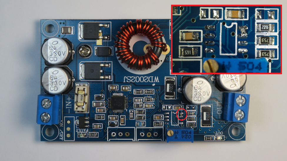
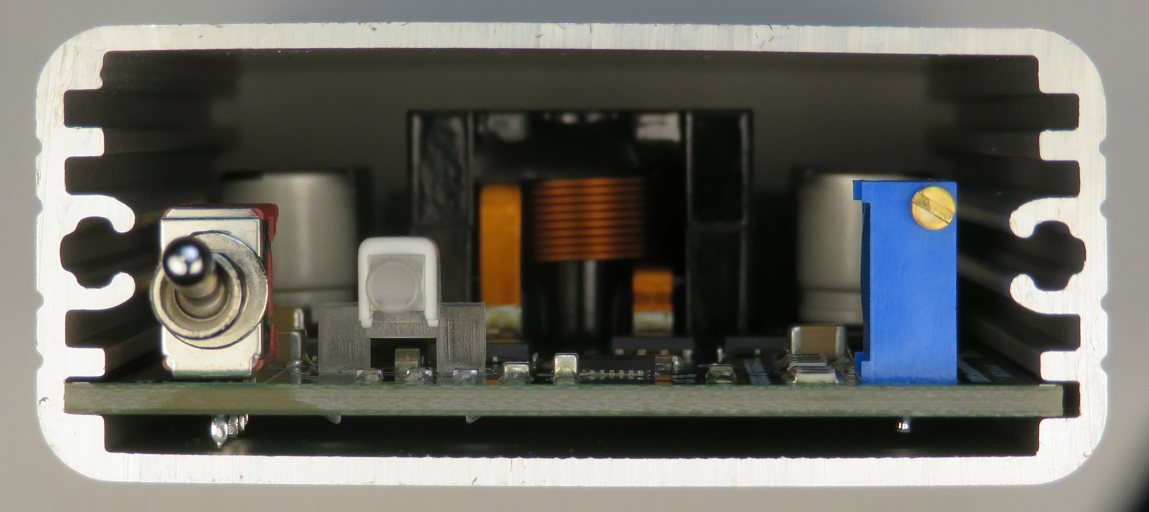
This board has been designed to fit into a Hammond 1455C802 Enclosure.
Design Considerations
The LT8390 is a synchronous 4-switch buck-boost DC/DC controller that allows the output voltage to be above, below or equal to the input voltage.
Not only does this provide an extremely flexible DC-DC converter, it is also ideal for battery operated systems where the battery terminal voltage can fluctuate depending upon the state of charge (SoC). For example, I have been using a similar DC-DC Buck-Boost converter with a QNAP NAS (Network Attached Storage) to obtain a stable 12.0V (as it directly feeds the Hard Disk Drives) from a 12V battery that could range anywhere from 10.8V to 14.4V.
The LT8390 operates in current mode and senses the current flowing through the inductor via the inductor sense resistor (R6).
When customising this design, please work through the calculations spreadsheet in conjunction with the datasheet.
Switching Frequency
The LTC8390 can operate with a switching frequency between 150kHz and 650kHz. Selecting a frequency is a trade-off between efficiency and component size. A low frequency converter improves switching losses but requires a larger inductor and capacitors. Switching at a higher frequency can reduce the overall size of the converter but comes at a compromise of efficiency through switching losses. I have selected mid ground, at 400kHz.
To improve EMI, the triangle spread spectrum frequency modulation scheme has been selected via R12. If you wish to switch this off, remove R12 and insert R15.
MOSFET Selection
A global shortage in power MOSFETs has meant we need to accept what is available from catalog companies at the time of purchase. As such, MOSFETs with a breakdown voltage of 60V were used in this design.
This breakdown voltage needs to be considered if you want to run the converter (input or output) at voltages approaching 60V. You would be wise to select 80 or 100V MOSFETs.
The gate drive voltage is generated by INTVCC (5V) and hence logic level FETs must be used.
Output Voltage
The output voltage is programmed using the R2/R4/R7/R8 voltage divider network. The LT8390 has a 1.00V feedback threshold on FB (pin 16). Provision has been made for a fixed output by populating resistors R2/R4/R8 or adjustable via a 10 turn trimmer (R7).
The LED is attached to the power good output (PGOOD). PGOOD is active when output is within +/- 10% of the set voltage.
Output Current
The LT8390 has provision for an input or output current sense resistor to limit either the input or output currents. If not used, the ISP and ISN pins can be shorted to VIN, VOUT or ground.
Limiting the input current could be useful in, for example, solar power applications to set the input current close to the maximum voltage at Maximum Power Point (Vmp).
Limiting the output current can be useful for charging batteries where a CC/CV profile is required. A depleted battery can start out in constant current (CC) mode, and switch to constant voltage (CV) once the set voltage has been reached.
Provisions for output current limiting was included in this design.
The LT8390 will throttle back when more than 100mV is detected between ISP/ISN, hence the 0.01 ohm shunt currently sets the maximum output current at 10A. This threshold could be further adjusted by a voltage on the CTRL pin (pin 10), however this is currently tied to VREF (2V) enabling 100% full scale output, i.e. 10A with a 0.01 ohm shunt.
As the output current sensor resistor has been placed before the bulk capacitors, some ripple current can be expected on the signal. R9/R10 and C16 can be used to filter this out.
Undervoltage Lockout
The EN/UVLO pin has a falling threshold of typically 1.220 volts with 13mV hysteresis. Additionally, when the voltage falls below 1.220 volts, this pin will sink 2.5uA providing additional programmable hysteresis by appropriately sizing R5.
Currently the under-voltage lockout is set at 11.5V, and won’t be re-enabled until the supply exceeds 12.2V. If required, the hysteresis window can be reduced by reducing R5 and then recalculating R3.
The front power switch (S1) is connected into the same EN/UVLO pin. When switched off via S1, the quiescent current will be typically 2uA plus the current though R3. I was observing a quiescent current of about 60uA @ 12V.
Laptop Leads and Connectors
Various DC power leads for laptop computers (and some Sony TVs) can be sourced from AliExpress or ebay. For example:
Design Files
Design files can be downloaded from the Circuit Maker website. Circuit Maker is a free EDA tool from Altium.
- Open in Altium 365
- LT8390 Calculations Spreadsheet (XLSX)
- LT8390 version 1.A.6 Gerbers (Zip)
- LT8390 version 1.A.6 Schematics (PDF)
- LT8390 version 1.A.6 Bill of Materials (XLSX)
The PCB for this design was fabricated by jlcpcb.com.
Hello Craig!
really nice PSU!
I really miss lack of higher quality synchronous DC/DC like this. We would like to use your design in your scientific instruments (non profit usage, for our own usage only).If you would like to know more, contact me at [address removed].
I have some questions:
1.) DO you thing that this design can handle output 5A load @ 28V or @ 30V ? I would add solid heatsing on bottom with fan.
2) I guess that current UVLO could be easily lowered to eg. 5V by only changing R3 and R5?
3.) Can we somehow send you some donation? 🙂
Regards,
Marek
Marek,
1.) I would be comfortable with an output of 5A @ 30V. The current is the main contributor to heat and I’ve had design at 6A. What input do you wish to use, as this may be the limiting factor. For example at 15V, the input current would be 10A.
2.) That is correct. If you don’t want the switch (S1), you could disable UVLO by removing R5 and putting a 0 ohm resistor in place of R3.
3.) Yes, donations are welcome and can contribute to further advancing the design (e.g. through the purchase of a 2nd version of the PCB or electronic components). Probably the easy way to donate is using Paypal to Craig.Peacock@beyondlogic.org (Please note this mailbox is unattended, but works for Paypal)
Regards,
Craig
Hi, have you measured the efficiency between power in and power out?
Is it close to the LT8390 datasheet stated up to 98%?
Thanks!
Rafe, to date I have done limited efficiency testing, but it has been pretty good.
I’ve simply picked two scenarios that I intend on using, rather than plotting it and cherry picking the best ‘sweet’ spot.
Both the DC load and power supply were wired in 4 wire mode, eliminating losses in the cables. (Photos are over in the Circuit Maker Gallery)
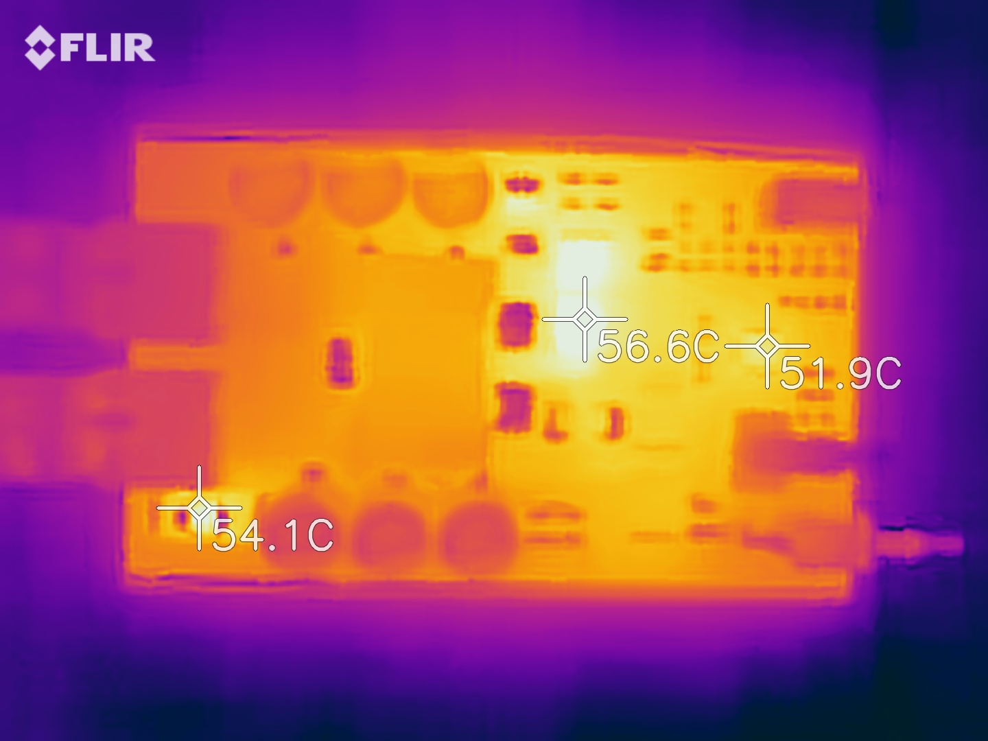
In Boost mode 12V input, 19.5V output @ 3A, efficiency is 95.6%
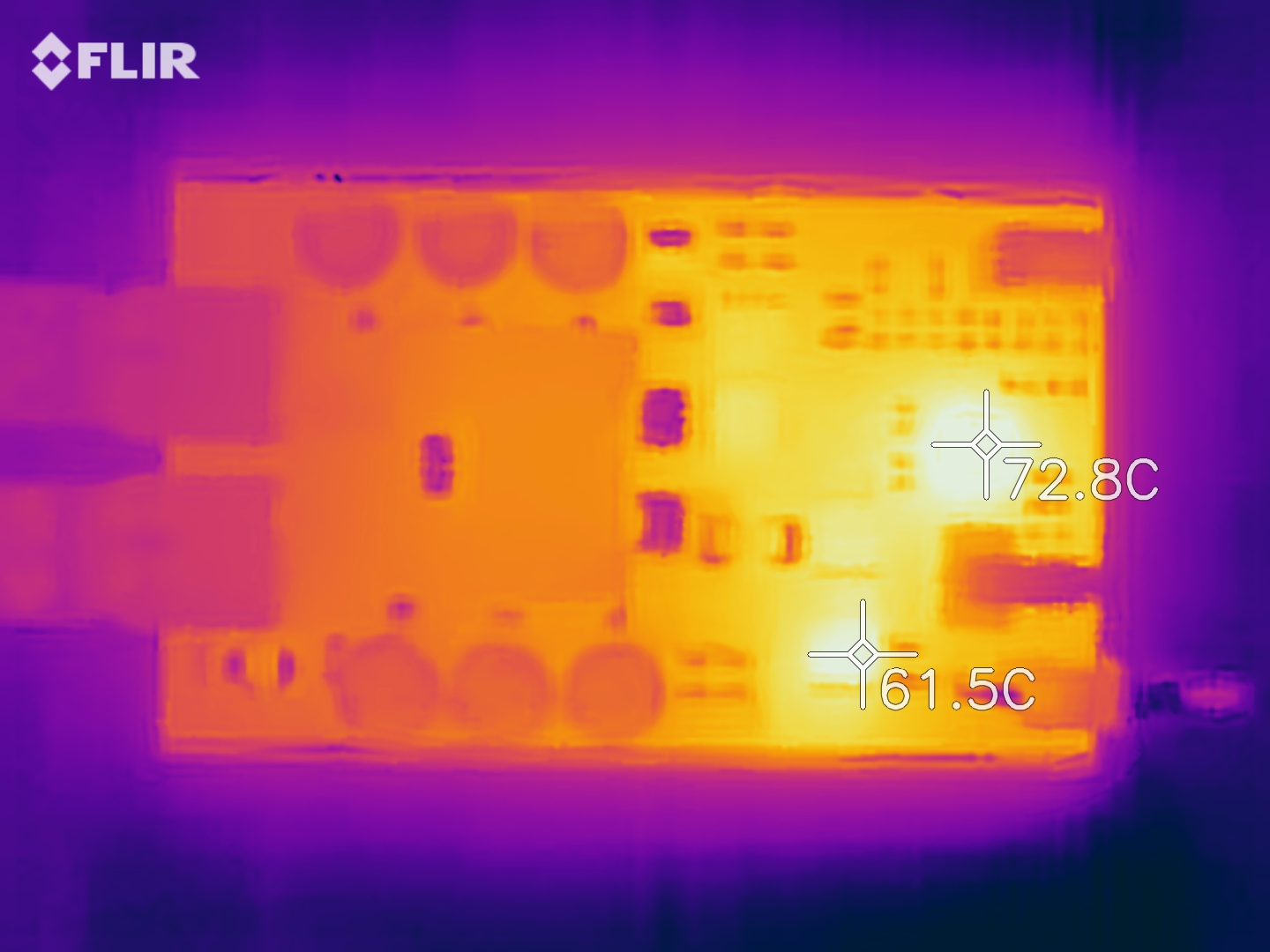
In Buck mode 24V input, 19.5V output @ 6A, efficiency is 96.7%
The design is missing optional Schottky diodes B and D that could help to further improve efficiency.
When (if) I get the time, I do have plans on programming the power supply and DC load to plot different voltage and currents efficiency curves.
Thank you, I did not see the photos.
Seems to be really efficient!!
hi Craig and co,
I have bought LTC3780 boards and had this experience; inputting from a 12V battery on charge and using the output to provide a constant current output to charge a lead crystal battery no problem. The required current output for first stage of the charge regime could not be met as it should be 0.3C on a 35A.hr battery hence 10.5A
I thought no problem I’ll use two boards in parallel, each set to 5.25A limiting and 14.7V. It soon resulted in one of the two heatsinks of one board getting really hot and by the time I’d pulled power the on-board fuse had blown. I thought perhaps I’d carelessly shorted something. I managed to get the board working by fitting an external fuse. Using the remaining board and another new one resulted in smoking hot heatsink. I think some feedback either on output or input drives them out of control. Don’t know what filter components could prevent this but thought I’d share. Might well relate to your issues with two boards sharing a source?
Hi,
nice work youve done there 🙂
Id really like to try this Board as a 12S Li ion Charging Solution. But one thing that keeps me away is the use of the QFN package. Im not sure if i could solder that in myself. I have a hotplate and a Heatgun, you think its easy with these tools? ^
How did you do it, did you solder the Parts by hand or have did a Assembly Service did this for you?
KidCe,
I ordered a stencil from the PCB fabricator at the same time I ordered the PCB. I then used solder paste and a SMD/BGA hot air rework station to put the QFN and the MOSFETs down. You should be able to do similar with a hotplate or hot air tools.
Hi, Thanks for the good info. I just purchased LT8391 demo board to do a battery charging. But Im lacking info of how the C/10 charging CC/CV works. Since FB pin voltage of 0.95Volts puts the mode to FLOAT it can not be adjusted by FB resistor network. So CV mode must start somewhere before that?
About the circuit with LM358 and the overvoltage on RUN pin. They simply made a mistake by allowing the pot to conduct Vin to LM358 input pin. Simply adding a series resistor to pot and 5V zener to LM358 input would do the trick.
Juha,
You don’t specify your battery chemistry, but generally for CC/CV Charging you would set the float voltage using the FB pin. You would then set the maximum current using the shunt resistor connected to ISP/ISN and the CTRL pin.
When a flat battery is connected to the LT8391, it will pull the maximum current set via the shunt resistor (Constant Current) until it reaches the float voltage (Constant Voltage).
It will be Li-Ion. It is quite clear as far as I can see from the datasheet. Shunt resistor determines the maximum current, CTRL pin is used to alter the maximum current by analog value under 1.35V i.e. analog dimming. In my case charging is started by analysing the battery voltage and balance to determine which current is good to start with so adjustment is used to not charge the totally empty battery with full amps.
Still the question remains, at which point the charger moves to CV mode, it cant be the FLOAT voltage limit set by FB pin since reaching that limit will immediately end the charging. As well it is seen in the datasheet page 31 where they show the CC/CV charging curve. Float voltage is reached way after the charger has moved already to CV mode. When FLOAT limit is reached FAULT(C/10) pin pulls low and charger goes to idle. They mentioned on some app note that C/10 is in built function..?, does that mean the CC/CV corner point is somehow fixed in relation to FB pin voltage… ?
I guess I have to test it with the evaluation board..
Isn’t the transition between CC/CV is determined by the battery? This is the point that that battery no longer accepts the full rate of charge current.
If that would be the case the whole point of having FB pin would be lost in a case where battery is wished to charge lower that “full”, it would never enter CV mode..
I bought the mentioned LTC3780 circuit, but the under voltage protection doesn’t work properly below 8V.
For my model it switches off at 6.5V for example, but when the voltage drops even more to 6V is suddenly starts working again (below the voltage limit!)
For higher voltages I don’t have this Problem. Can you please set it to 6.5V and test yours?
The wiki is can’t open.
I wonder how this compares to the 12V 15A step down ($60 CAN!)? I was hoping to stuff more batteries into my drone